制作EUV:从实验室到工厂
将ASML的合作旅程盖起来,将极端紫外线(EUV)的光刻技术推向市场。万博manbetx官网登录
9分钟阅读 -桑德·霍夫曼(Sander Hofman),2022年3月30日
四十年,在研发中,一项重要的合并,全球成千上万的人:将EUV光刻带入大量制造业是一项巨大的努力。了解在启动ASML第一个EUV系统的途中发生的关键时刻,以及对下一步的瞥见。
EUV的黎明
EUV故事始于1980年代中期日本,届时,基于70年代在俄罗斯进行的多层镜研究,Hiroo Kinoshita投影了第一张EUV图像。美国和荷兰的实验室很快也开始探索这一潜在的光刻发展发展。最初称为“软X射线”光刻,名称“极端紫外线”的灵感来自天文学家使用的术语,用于相同的光波长和光子能量。
在光刻中,使用较短的光波长使芯片制造商能够缩小大小并增加芯片上特征(或晶体管)的密度,从而使芯片更快,更强大。当ASML成立于1984年时,该行业正在使用汞蒸气灯,该灯产生了436纳米(NM)的光,称为G线,后来是365 nm的紫外线(UV)光,称为I-Line。早期的EUV研究人员追求了几个从4到40的波长,但最终以13.5定居为使用锡血浆产生EUV光的最佳位置。
EUV wasn’t the only technology that researchers explored to enable future generations of ‘shrink’. Electron beam lithography and ion beam lithography seemed to be other viable options, but ASML placed an ‘educated bet’ on EUV lithography, because it was the technology that seemed best suited to continue transistor scaling while remaining affordable in mass production.
Not everyone was immediately sold on the idea of EUV technology, however. At a2020 SPIE conference retrospective当时曾在NTT的研究员Hiroo Kinoshita描述了说服他的科学家认为EUV光刻有机会的挑战。他说:“ [我的结果]在1986年日本应用光学学会的年度会议上。”“不幸的是,观众对我的演讲非常持怀疑态度。但是,我的信念没有改变。”
劳伦斯·利弗莫尔国家实验室(Lawrence Livermore National Laboratory)的长期半导体行业资深人士和当时的研究员安德鲁·霍里卢克(Andrew Hawryluk)回忆起会议上的类似挫败感。他解释说,1987年12月,一位教授如何来拜访他和他的团队。在了解了他们在EUV中的开创性研究之后,教授问:“但是您真的可以对这些事情做任何有用的事情吗?”
“他的话困扰着我,”安德鲁说,安德鲁在圣诞节休息回家,两周后返回了30页的euv光刻。他和他的团队在当年晚些时候的一次会议上介绍了该论文,但即使那样,很难找到支持。安德鲁回忆说:“你无法想象我在演讲中得到的负面接待。”“观众中的每个人都会使我束缚。我的尾巴在两腿之间回家,誓言再也不会谈论EUV光刻了。”
但是一周后,安德鲁(Andrew)接到了贝尔实验室的威廉(比尔)布林克曼(Bill)布林克曼(Bill)布林克曼(Bell Brinkman)的电话,后者随后成功地让美国能源部在劳伦斯·利弗莫尔(Lawrence Livermore)和桑迪亚(Sandia)实验室为国家的EUV光刻研究计划提供资金the ‘Virtual National Laboratories’.
致力于工业化
“Bill got us the money, but the money was going to run out sooner or later,” said Andrew. “What was absolutely critical was to get the industry involved to support this new technology.”
安德鲁(Andrew)的老板,已故的纳塔尔(Nat)塞格利奥(Nat)塞格利奥(Nat),在招募公司来拥抱包括英特尔在内的EUV方面发挥了重要作用。
参与的美国芯片制造商成立了“ EUV LLC”,该公司与虚拟国家实验室签约,以加速EUV光刻发展,并降低与新技术工业化相关的风险(EUV光刻,Wurm,Stefan,Stefan,Gwyn和Chuck,2008年)。万博manbetx官网登录

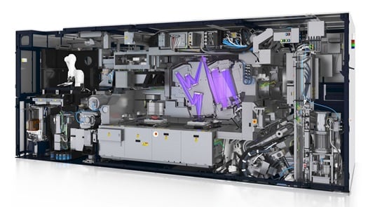
ASML的原型EUV系统之一或“ Alpha Demo”工具。
Meanwhile, in the Netherlands, Fred Bijkerk, a professor of EUV optics, projected the first EUV images in the Netherlands in 1990. It wasn’t until the late 1990s, however, that research into the industrialization of EUV lithography began in Europe. In 1997, ASML brought in Jos Benschop (senior vice president of Technology) to kick off our EUV program.
在乔斯的帮助下,1998年,ASML与我们的长期合作伙伴The Derman Partners The Derman Partners The Derman Partner The Derman Partner The Derman Partner The Derman Partner The Derman Partner The Derman Partner The Derman Partner The Derman Partner The Derman Partner Shusturors Zeiss和Synchrotron Light Suilt Superion供应商Oxford Instruments成立了欧洲工业研发联盟(Extreme UV概念光刻开发系统)。ASML还与其他供应商合作,包括Philips Research和CFT,TNO-TPD,Fom-Rijnhuizen,PTB(德国国家计量学院)和Fraunhofer-IWS。ASML和Euclides于1999年与美国EUV LLC联手,而日本pursued EUV technology development通过其ASET计划(超级高级电子技术协会)和后来的日本极端紫外线光刻开发协会(EUVA)计划。
In 2000, Jos was able to present the EUCLIDES program’s first results at SPIE. Having seen what was possible, in 2001 ASML assigned a small group of people and modest resources to build a prototype EUV system.
The team achieved their goal in 2006, when the first EUV prototypes were shipped to imec in Belgium and SUNY (College of Nanoscale Science & Engineering) in Albany, New York. There, the prototypes were used to better understand EUV and how this new technology could fit into the semiconductor manufacturing process. Things were starting to get real.
实现“第一光”
在2008年春季,SUNY使用其演示工具生产世界上第一个全场EUV测试芯片。在2009年,ASML开设了建筑物,这些建筑物将在荷兰Veldhoven的总部容纳我们10,000平方米的清洁室和工作区,用于EUV开发和生产。
然后,在2010年,我们将第一个Twinscan NXE:3100(预生产EUV系统)运送到了韩国的三星研究机构。该机器在圣诞节前夕获得了“第一光”(天文学参考)。对于乔斯来说,这是13年辛勤工作的高潮。

庆祝2010年首次EUV系统发货。
他说:“我们于1997年开始从事这项工作。”“突然之间,是2010年,您正在海外飞往韩国。您乘坐长途出租车,换衣服,去工厂[工厂],转弯,然后是:机器。那是一个很好的时刻。最初的梦想成为客户工厂的现实。”
这是一个很棒的时刻,但是仍然花了九年的时间才开始发布包含EUV技术的产品。万博manbetx官网登录乔斯解释说:“机器基础知识在那里,但是我们努力实现客户为使EUV成为负担得起的选择所需的生产力。”“It’s important to remember that the R&D phase at our customers also takes time,” says Jos. “After EUV’s ‘launch’, it still took one or two nodes for chipmakers to mature the technology and learn how to use it fully before commercial products could be built with it.”
该过程花费很长时间的部分原因是芯片制造商必须优化围绕新技术的基础架构。万博manbetx官网登录“在扫描仪旁边,您需要优化诸如标线师和光线师之类的东西,以及EDA(电子设计自动化) -the software toolsthat you use to design a chip, making use of the full benefit of the new capabilities. It’s a constant feedback process, with data from each part of the process influencing the others,” Jos explains.
2012年,我们的主要客户Intel,Samsung和TSMC同意在五年内为我们的EUV研发做出贡献,作为我们客户共同投资计划的一部分,以回报获得公司的股份。万博苹果手机客户端我们向亚洲和美国的不同客户运送了六个系统,并在2013年发货了第一个EUV生产系统 - Twinscan NXE:3300 - 向这项新技术开发的又一步。万博manbetx官网登录
万博manbetx官网登录一路上的技术挑战
“It took longer and was much more work than I imagined,” says Jos, looking back on the process. “You could say that we were either brilliant or just stubborn,” he laughs.
To make the jump to extreme ultraviolet light of 13.5 nm required innovations in practically all areas of the lithography machine, including the light source, the optics that shrink and focus the light onto the silicon wafer, and the reticle containing the blueprint of the chip to be printed. To make matters more complicated, EUV light is absorbed by almost everything, so it has to be produced and used inside a high vacuum environment. “The whole switch to vacuum was quite an adventure,” Jos recalls. “It made the materials a challenge due to outgassing – what materials you could use and how you had to handle them and clean them.”
乔斯解释说:“当Zeiss表明它可以使EUV光学元件成为专门的EUV光学时,我们的研究确实受到了关注。
然后,ASML的重点转向解决“来源”挑战。乔斯承认:“由于来源,我们受到了很多公众的殴打。”“多个客户会提及我们的源路线图,并说,这是您几年前承诺的,现实远不及它。他们实际上是在SPIE中钉死了我们。”
在2000年代初期,ASML开始与荷兰,日本和美国的EUV来源的几个潜在供应商合作,包括总部位于San-Diego的Cymer。ASML选择使用Cymer的解决方案,后来在2013年收购公司。但是研发比预期的要难得多。万博苹果手机客户端设计激光生产的等离子体(LPP)源涉及每秒50,000次的锡液滴(两次),以使它们蒸发,从而使血浆比太阳表面高40倍,以发出EUV光。
“We actually had some early success, and things looked pretty promising, and we thought maybe this is not as hard as we expected!” says Danny Brown (head of EUV Source System Engineering & Research). “And boy, we were wrong.” The main challenge was achieving 250 W of power in a full-scale demonstration source vessel. Despite many setbacks, the team working on it eventually succeeded and went on to获得Berthold Leibinger创新奖2021年9月。

在Cymer EUV光源容器中实现250 W的功率。
EUV在这里留下来
在我们的源头达到250 W(这使工厂吞吐量为每小时125晶片)并将其化为工业之后,隧道的末端就在眼前。根据乔斯(Jos)的说法,我们终于感觉到我们的EUV计划成功的地步是在2018年,当时我们的客户开始在其工厂中投入大量投资。万博manbetx官网登录“他们花了数十亿美元的建造晶圆厂并购买我们的机器,这表明他们真的相信EUV。”
In 2019, the首先支持EUV的商业产品was released (Samsung’s Galaxy Note10 and Galaxy Note10+ smartphones). In December 2020, ASML celebrated the 100th shipment of an EUV system, and as of the end of 2021, 127 latest-generation EUV machines were in use at customer locations around the world. “It took a long time, but EUV is taking over the critical layers for Logic as well as DRAM Memory,” explains Jos. “The best moment in my career was in 2019 when I spoke at a workshop – I got my Samsung smartphone out and said, ‘I once said naively that EUV would be in volume production in 2006. I shamefully admit that it's 13 years late,’ but then I waved my phone and said, ‘but some of you thought this thing would never exist.’”

ASML于2020年12月运送了第100台EUV机器。
下一步是什么?EUV 0.55(高NA)及以后
In our quest to enable ever-smaller chip features, we continue to innovate and are now increasing our EUV machines’ numerical aperture (NA) from 0.33 to 0.55, which means that the optics in the new systems will allow light with larger angles of incidence to hit the wafer, giving the system a higher resolution and decreasing the size of the features that can be printed. “Because this new lens is fundamentally different, it meant that we had to come up with a completely new way of manufacturing it and measuring its features,” explains Jos. “Our teams at ZEISS and in威尔顿打破了一个世界纪录。”计划在2023年底将EUV 0.55“ EXE”机器送给客户的研发目的,我们希望它们在2025年将在高量制造中使用。
但是在2022年,我们最大的挑战是每年将EUV系统的生产从40个系统增加到60个系统。EUV工厂副总裁Sheila Leenders表示,雇用更多的人并建造更多的洁净室空间只是问题的一部分 - 据我们EUV工厂副总裁Sheila Leenders称,困难的症结在于增加供应商网络的容量以满足EUV机器的需求。她说:“我们的供应基础正面临着一生的挑战。”“我们正在努力帮助他们提高能力并提高全球供应商需要的可靠性。”
通过合作克服挑战
多年来,ASML推动了许多挫折,意外的挑战和延误。但是乔斯说,每当他们看到新的挑战临近时,他们总是对如何解决问题有想法。乔斯说:“通过我们可信赖的合作伙伴网络,我们总是找到解决方法的方法。”
他继续说:“我们通过协作网络工作的方式是通过协作网万博manbetx官网登录络来工作。”“这使我们能够利用可用的知识并以'可接受'的风险状况进行进步。”
在EUV技术开发的所有阶段 - 研究,工业化和现在的大批制万博manbetx官网登录造业 - 在边界之间共同努力。Today, we procure some critical EUV modules from the US, such as the droplet generator for the light source as well as sensors, reticle handlers and stages, and other modules from Germany, such as our ZEISS optics and TRUMPF’s lasers for the EUV source, and we collaborate with companies and institutions all over the world in continued R&D for the next generation of EUV machines. Acting as the system architect at the center of things, ASML succeeded in building and mobilizing a global ecosystem to industrialize what many considered to be impossible technology. And we’re now confidently taking it into high-volume manufacturing.
想在ASML上发现有关EUV的更多信息吗?
About the author

- 桑德·霍夫曼
- 媒体关系经理
- 桑德(Sander)喜欢在ASML的数字渠道万博manbetx官网登录上将技术,故事和媒体融合在一起。他白天是一个通讯家伙,晚上有抱负的编剧,也是一个怪胎。